Wednesday 23 November 2016

ESR Project Build - Part 5 - Test Readings

With the opamp section soldered up and tested, I found that the range was a bit wider than I wanted. The designed range was good if you want to test down to 1 uF. However, to see more meter movement down near the 1 ohm range, I found that I could put a 47 ohm resistor in parallel with the 10 ohm resistor at the DUT terminal. This expands the scale near 1 ohms slightly, so that the readings vary between about 1 and 4 ohms. I plan to make this a "fine" switch setting on the finished meter assembly.

With the setting on "fine" you can measure about 100 uF and higher. Any caps below that, will read off scale (to the left). Turning the switch off (coarse), the unit does measure 1 uF and up.

Figure 1 below shows the Sencore transistor testor 100 uA meter that I used in the zeroed position (right).
Figure 1. ESR meter in zeroed position.
The remaining figures are readings while the switch is on "fine" at various resistances.
Figure 2. 1 ohm
Figure 3. 2 ohms
Figure 4. 3 ohms
Figure 5. 4 ohms
From these readings, you can see that on "fine" that the resistances spread out rapidly. With the switch set to coarse, 10 ohms reads about where figure 5's 4 ohm reading is. Then anything higher bunches to the left of that.

For switching power supplies where the capacitors are expected to have milliohm values of ESR, the "fine" setting should be suitable for identifying failed caps. It is still not the best arrangement for cherry picking caps because of its inability to read milliohm differences.

Later when the hardware build of the cabinet is done, I'll add some photos to the last part in this series. Thanks for reading!

Monday 21 November 2016

ESR Project Build - Part 4 - Precision Rectifier + Meter

We've so far looked at the ~100 kHz oscillator, driver and gain stages. After the gain stage comes a precision rectifier and driver, which looks like this (Figure 1):

Figure 1. The Precision Rectifier and meter driver
I decided to breadboard this portion since I am substituting the LM358 for the AD8032, which the W2AEW design called for. The AD8032 is a bit pricey and harder to obtain (Mouser price for DIP was $8.11 US in single quantities). The AD8032 is a rail-to-rail opamp but this circuit only requires the bottom rail to function correctly.

The LM358 is a jelly bean part and operates at the V- rail (ground in this case). This part is targeted as a single supply solution. As a bonus, it uses the same pinout as the AD8032. The one other deviation from the W2AEW design is that my selected meter has a 100 uA movement instead of 200 uA. So instead of the 4.7k + 2.2k with 10k adjustment pot, I simply ran the output signal into a 100k trimpot (for this breadboard test), with the other leg of the pot going to ground. Then the meter went to the wiper arm of the pot with its negative lead going to ground. The full deflection is adjusted with the DUT leads shorted. In the final soldered up build, I'll arrange a protective limiting resistor for the meter in case the pot gets cranked.

The signal coming out of the LM358 precision rectifier and going into the driver (pin 5) appears as shown in Figure 2:
Figure 2. Input signal at LM385 pin 5

It is interesting to see that the signal actually does dip below ground by -590 mV. The positive swing of the signal goes up to 650 mV. This signal is generated when the DUT leads are shorted (zero ohms).

With the 1N4148 diode and the 0.1 uF filter cap connected, a DC voltage is established, which is then delivered to the meter. To calibrate, short the DUT leads and adjust the pot to give the meter full deflection like the old fashioned ohm meters.

Early testing has shown that low ESR values show very close to the shorted leads point on my meter. Any resistance over an ohm shows as a reading near the 10% deflection point. So presently, I found this meter to be extremely ESR sensitive.

Once you have a hammer, everything looks like a nail. So I went around the lab looking for caps to measure. All but one measured 100%. This failed cap was pulled out of an '80s power supply along with three others just like it. I had been debating whether or not to use these or to replace them in a power supply project. One of the four showed no deflection at all, while the remaining three all showed 100% good.

I also in-circuit tested this circuit on Intel Atom motherboards with caps and measured a few other boards. All indications look very good so far. Now I just need to find some time to solder this up in its final form.

In the next part, I'll present some pictures of my build into an old Sencore transistor tester case.

Sunday 20 November 2016

ESR Project Build - Part 3 - Amp

In the amplifier input chain, we first encounter the DUT filter cap (0.1uF) and load resistor (100 ohms). This test signal conducted through the test capacitor is then AC coupled to the amplifier stage.
Figure. Device Under Test input

Amplifier


The amplifier Q1, is suggested as any general purpose signal transistor like the 2N2222 or 2N3904 etc. I chose the latter, though I had ready access to both. Figure 2 shows the basic common emitter amplifier configuration used.
Figure 2. 2N3904 Amplifier stage
The 100 ohm resistor in the emitter leg adds negative feedback and reduces the overall gain of the circuit. The input signal is coupled in with the 0.01 uF cap and then coupled out of the collector circuit with another 0.01 uF circuit.

This circuit should have been painless to add to the existing prototyped circuit, but try as I might to get the orientation of Q1 right, I got it backwards! Doh! After snipping out the failed part and replacing it with another with the correct orientation, the gain came up to what it should be (a transistor with emitter and collector reversed will still function but with low gain). Figure 3 illustrates the pinout for this device.

Figure 3. 2N3904 Pinout
The output of the amplifier stage taken from the collector's coupling capacitor is shown in Figure 4.
Figure 4. Amplifier stage output (at collector)
Here we can see that the output is 640 mVpp, with the DUT probes shorted (for zero ohms). Going out of the oscillator driver, I measured about 355 mVpp. With DUT probes shorted and the signal appearing across the 0.1 uF filter cap and 100 ohm resistor the signal coming in is about 157 mVpp (Figure 5).

Figure 5. Input signal arriving from DUT.
So if the input signal is 157 mVpp and the output voltage from Q1 is 640 mVpp, then this would represent an overall voltage gain of about 4. But don't forget that the stage also adds power gain.

Next up, we'll review the precision rectifier stage.

ESR Project Build - Part 2 - Oscillator

The basis of the tester starts with a 100 kHz oscillator circuit. The two designs are similar, but I'm building based upon the W2AEW circuit:

The oscillator consists of a pair of CD4049 inverters biased to oscillate. The remaining four hex inverters are used to drive the signal into a 10 ohm resistor. This produces the signal sent to the Device Under Test (DUT) with enough power, but low enough in voltage to avoid silicon diode conduction.

The scope trace in Figure 1, shows the oscillator signal when the circuit was powered from about 6 Volts. The rise and fall times are 80 ns and the duty cycle was about 55%.

Figure 1. Oscillator output (before drivers)
Figure 2 illustrates the output signal out of the driver stages into the 10 ohm resistor. The voltage drops to about 355 mVpp and the frequency rose to about 119 kHz. With the driver attached, there was less load upon the oscillator stage. At these lower voltage levels, you can see more of an influence from the inductance side of things in the trace output.

Figure 2. Driver stage output into 10 ohms.
Getting the oscillator to work was fairly painless. Because I am prototyping this, I always run the risk of solder blob shorts and this time was no exception. After elimination of a supply side short and then another solder blob affecting the oscillator circuit, the circuit took off with no trouble.

In the next part, we'll look at the receiving side of the DUT probes.

ESR Project Build - Part 1 - Designs

I wasn't planning to blog this project, but it has turned into quite a bit fun, even though at the time, it seemed to be small project. As is so often the case, even the small projects provide challenges.

Why?

Many things today stop working due to switching power supply problems. Let's face it, switching supplies work hard at converting power and the capacitors involved usually fail at some point. Monitors and TVs etc. can often be fixed by just replacing the faulty caps.

But identifying the failed caps is not always easy. Many times you have a bulged or other obviously marked cap. But at other times, you may have parts that are border line, which are difficult to identify. 

No one wants to remove caps to test them on an ESR meter. So when I went hunting for a design, I wanted the following:
  1. Must work in-circuit
  2. Be relatively simple to build
So in my research, I came across the following two designs:
I believe the W2AEW design is based upon the VE7IT design. 

Designs


The VE7IT tester produces a small 156 kHz signal of about 250 mVpp, to stay under the silicon diode conduction voltage of about 0.6V. While a Schottky diode conducts between 150 to 450 mV, am hoping that this doesn't apply often or interfere too much when it does. The VE7IT design says the cap being tested must be greater than 1 uF. Fair enough.

The signal returned from the DUT pair of probes in the VE7IT design, is then AC amplified by a 2N2222 stage and rectified by a bridge rectifier.


After the rectification, the circuit drives a 50 uA meter with a potentiometer for zero adjustment.

A note on the VE7IT schematic indicates that:
"There is no DC output until approx 75-100 ohms of ESR is seen at the test terminals (like a bad cap). Mid scale is approx 10 ohms. Full scale is 0 ohms."
As a rough measurement this is ok I guess, but I wanted to be able to measure down to the ohm if possible.

The W2AEW circuit substitutes a precision rectifier instead, so that greater precision can be had:


This should permit a finer resolution of readings from zero to 75 ohms that the VE7IT design is unable to read.

The other aspect of this design that I liked is that due to the opamps, it is no longer confined to using a 50 uA meter movement.

In the next part, I'll describe my own experiences with the build of the W2AEW circuit starting with the 10 kHz oscillator.

Tuesday 1 November 2016

Reverse Engineering: PC1031-0B Part 4

In the last post, I walked through the tracing of the serial data that loads into the shift registers IC1 through IC3, as well as described how IC4 was used (NOR gate). But there is one more shift register IC5 CD4021, which hasn't been analyzed.

CD4021

The functional NXP diagram is shown in figure 1.  There is a DS (serial data in), CP (clock pulse), outputs Q5, Q6 and Q7. And then there are parallel load inputs D0 through D7, with a parallel load signal PL.  This screams parallel load of push button data and then shifted out.
The first hunch here is that the CP signal (clock) is shared with the other shift registers. A resistance reading confirms this, so no mystery there. The parallel load (PL) is probably wired up to the strobe signal, since there is only one remaining signal left for the PCB and it has to be for the shifted out data. A meter reading confirms that PL is connected to the strobe input on the board.

The D0 through D7 inputs connect to the pushbuttons and are loaded when the board Strobe goes high. After the Strobe returns low, successive clock pulses (CP) shift out the data (PCB pin 2, green wire).

The only remaining question, which is fairly obvious actually, is where does the shifted out data come from?  It has to be be Q7 or else one or more bits would never be seen at the PCB pin 2 output. A simple resistance reading confirms this, if there was any doubt.

So now we have decoded the PCB connections:
  1. +5 Volts (purple wire)
  2. Push button data out (green wire)
  3. Data in (yellow wire)
  4. Strobe in (red wire)
  5. Clock pulse in (orange wire)
  6. Ground (brown wire)
After programming the AVR device (ATmega328P), I was eventually able to drive this board with a few mis-steps. Essentially, with the PCB mod (more about this later), I shift out 25 bits of data and then strobe it. The DLG modules that have the low /WR signal going high, then receive their data. At the same time, the Strobe signal enables any push button LEDs, when in the low state (these are active low). Finally, after the Strobe returns low, a few more clock pulses (CP) return the push button data (the button data is loaded at the high of Strobe). The AVR code can be found here:


CD4001 Hack

One major irritation with the PCB was that it limited access to the DLG-1414 character set. The PCB would play games with data bit D6 via IC4a.  I tried to find ways to use the PCB unmodified and gave up on that. Since only the first gate is used in IC4, we can just pull the chip out entirely (the board functions without it).  By soldering a wire from pin 3 of IC4a to pin 10 (QS2) of IC3 as described in part 3, we arrive at full control of D0 through D6 of the DLG-1414.


The Schematic

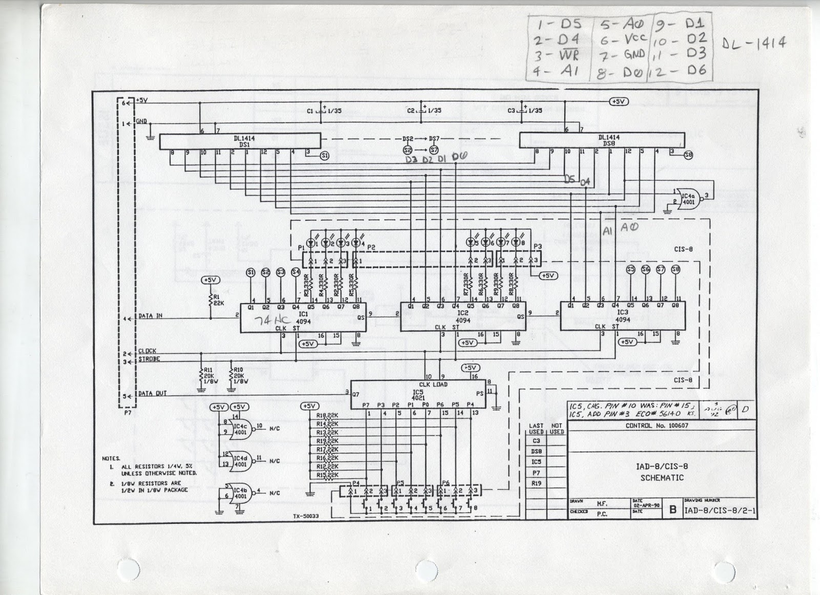
I was later reminded that I did in fact have a schematic for this PCB. So let's look at it now (Figure 2), to see how we did.

Figure 2. The PCB Schematic
The first thing I noticed was that they numbered their connections opposite to the way I did mine. Their pin 6 was my pin 1 for +5 Volts. Otherwise, things were fairly accurate.

Their wiring of IC4a was different than mine. As discussed in Part 3, I had a resistor divider, while the schematic shows pin 2 grounded and pin 1 connected to pin 1 of the DLG-1414. With IC4 removed and the mod added, this is all academic now.

My particular PCB also disagreed about the push button wiring. I was required to map the buttons as follows:

    struct {            // Input order
        unsigned pb4 : 1;
        unsigned pb3 : 1;
        unsigned pb2 : 1;
        unsigned pb1 : 1;
        unsigned pb7 : 1;
        unsigned pb6 : 1;
        unsigned pb5 : 1;
        unsigned pb0 : 1;
        unsigned fill : 8;
    } sr;    

So there you have it. I hope you enjoyed this little journey down reverse engineering row!